
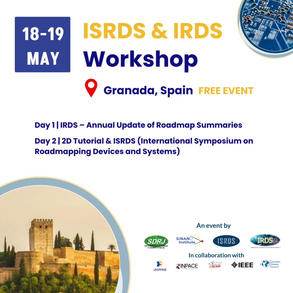
2026 IRDS/ISRDS Workshops
in Granada on 18-19 May 2026!
During two days, experts will present the latest update of main IRDS chapters, and discuss new direction in computing, and new directions of materials & devices for computing.
Day 1 – IRDS – Annual Update of Roadmap Summaries
Day 2 – 2D Tutorial & ISRDS (International Symposium on Roadmapping Devices and Systems)
IRDS represents the main International Roadmap of the Electronic Industry. The main challenges and possible solutions covering materials, devices and systems for many applications in the next 15 years will be highlighted.
The ISRDS will be dedicated to new direction in computing, including neuromorphic, probabilistic, reversible, and quantum computing, and new directions of materials & devices for computing, including 2D and ferroelectric materials, steep slope devices, quantum materials and devices, spintronics and cryogenic electronics.
Assembly Hall of the Faculty of Medicine Tower B, Floor 1 University of Granada PTS Parque Tecnológico de la Salud Avda. Doctor Jesús Candel Fábregas 11, 18016 Granada
Programme
Day 1 : 18 May
- 9:10-9:40
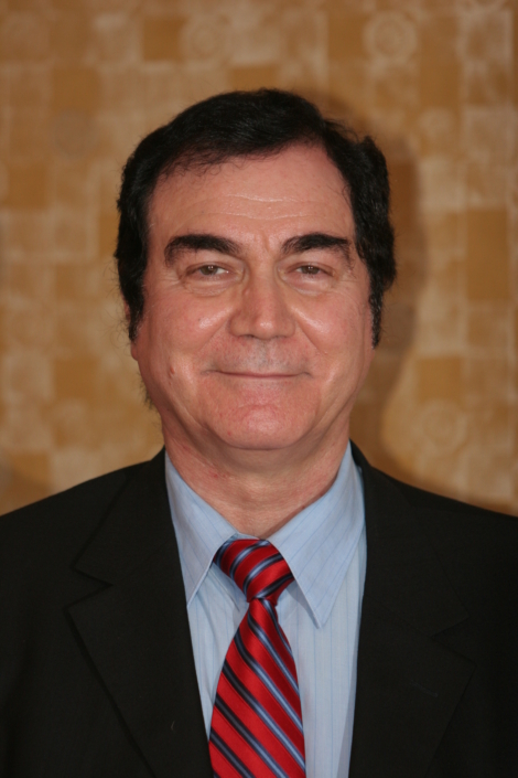
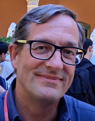
IRDS Introduction - Paolo Gargini
Bio
Paolo Gargini
In the 70s Dr. Gargini was a researcher at Stanford University and at Fairchild Camera
and Instrument. In 1980 as manager of MPU technology at Intel transferred into
manufacturing the iconic 80286 and 80386. In 1996, he became Director of
Technology Strategy and responsible for worldwide consortia research until 2012. He
was a member of Sematech, SRC, EUV LLC, EIDEC, ASET, IMEC and SIA Boards, and
Chairman of the I300I and NRI. From 1998 to 2015, Dr. Gargini was Chairman of the
ITRS sponsored by the WSC. Since 2016 he is the Chairman of the IRDS sponsored by
IEEE.
- 9:40-10:10
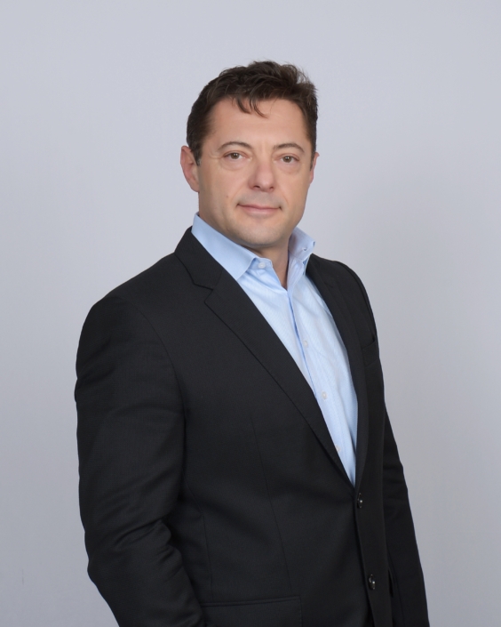
Yield Enhancement (YE) - Slava Libman, FTD solutions
Abstract
This presentation focuses on recent developments in Yield Enhancement, one of the most critical areas enabling advanced semiconductor manufacturing. The Yield Enhancement forum and its associated initiatives incorporate contributions from team members across the United States, Europe, and Japan. The scope of Yield Enhancement prioritizes contamination control challenges, for which solutions often require many years to develop and mature. Over the past year, much of the work has focused on advancing the understanding of defectivity in next-generation devices, informed by extensive collaboration between the Yield Enhancement and More Moore teams.
Bio - Slava Libman
Dr. Slava Libman is Chief Executive Officer of FTD Solutions, a company advancing digital platforms for water management and environmental performance in industrial operations. He brings three decades of experience in water technology, with deep expertise in the semiconductor sector across technical, operational, and executive leadership roles. Dr. Libman serves as Co-Chair of the semiconductor technology roadmap, where he leads initiatives in Environmental Sustainability and Yield Enhancement. He is also involved in the development of industry standards in these domains and organizes technical conferences and webinars that shape cross-industry collaboration. Prior to co-founding FTD Solutions, Dr. Libman held senior roles at a leading semiconductor manufacturer, a global architecture and engineering firm, and a premier analytical laboratory. He earned a Ph.D. in Environmental Engineering from the Technion – Israel Institute of Technology.
- 10:10-10:40
Applications, Systems & Architectures (ASA) - Vladimir Getov, University of Westminster
Abstract
Since the IRDS inception in 2017, the Applications Benchmarking (AB) and Systems and Architectures (SA) International Focus Teams (IFT) have contributed the tops down guidance to the IRDS communities. AB shared insight into what we need to compute and tracked the capabilities of systems to achieve those needs while SA provided insight on where that computing occurs across system categories from IoT Edge beacons to exascale supercomputers. The rapid adoption of generative AI has provided an unprecedented stochastic shock to the entire IT ecosystem, which demands changes to our methodology and has led to the merger of the two teams.
Bio - Slava Libman
Vladimir Getov is a professor of distributed and high‑performance computing at the University of Westminster and an active IEEE Computer Society volunteer since the mid‑1990s. He has served on the IEEE CS Board of Governors and contributed to both the Publications Board and the Technical and Conference Activities Board. He has held numerous leadership roles, including area editor for Computer since 2008 and chair positions for several IEEE conferences. His career spans industry and academia, with early work in computer development and later academic appointments in Southampton and Westminster. He has played a key role in international initiatives such as the PARKBENCH Committee, the Java Grande Forum, and the Open Grid Forum. Getov has received multiple prestigious awards and is a Senior Member of IEEE and ACM as well as a BCS Fellow.

Coffee break
- 11:10-11:40
Autonomous Machine Computing (AMC) - Jean-Luc Gaudiot, UCI
Abstract
Robotic workloads are fundamentally characterized by continuous sensor streams, sparse and irregular computation, tight perception–action loops, and strict real-time and energy constraints. This AMC roadmap update focuses on the core message that dataflow architectures are uniquely well suited to these demands, as they enable event-driven execution, fine-grained parallelism, and locality-aware computation across heterogeneous sensing, learning, and control pipelines. By aligning computation with data availability rather than instruction sequencing, dataflow architectures offer superior scalability, energy efficiency, and responsiveness, making them a critical enabler for autonomous machines operating in dynamic, real-world environments under the IEEE IRDS framework.
Bio - Jean-Luc Gaudiot
Jean‑Luc Gaudiot is a Distinguished Professor of Electrical Engineering and Computer Science at the University of California, Irvine. He previously served as Professor at the University of Southern California and later chaired the EECS Department at UCI, where he led significant growth and faculty recruitment. He is the recipient of the 2026 Richard E. Merwin Award for Distinguished Service. He has held major leadership roles within the IEEE and the IEEE Computer Society, including serving as President of the IEEE Computer Society in 2017. His research focuses on parallel system programmability, hardware‑based computer security, and autonomous driving systems, with nearly 300 refereed publications. He was elected IEEE Fellow in 1999 and AAAS Fellow in 2007.

- 11:40-12:10
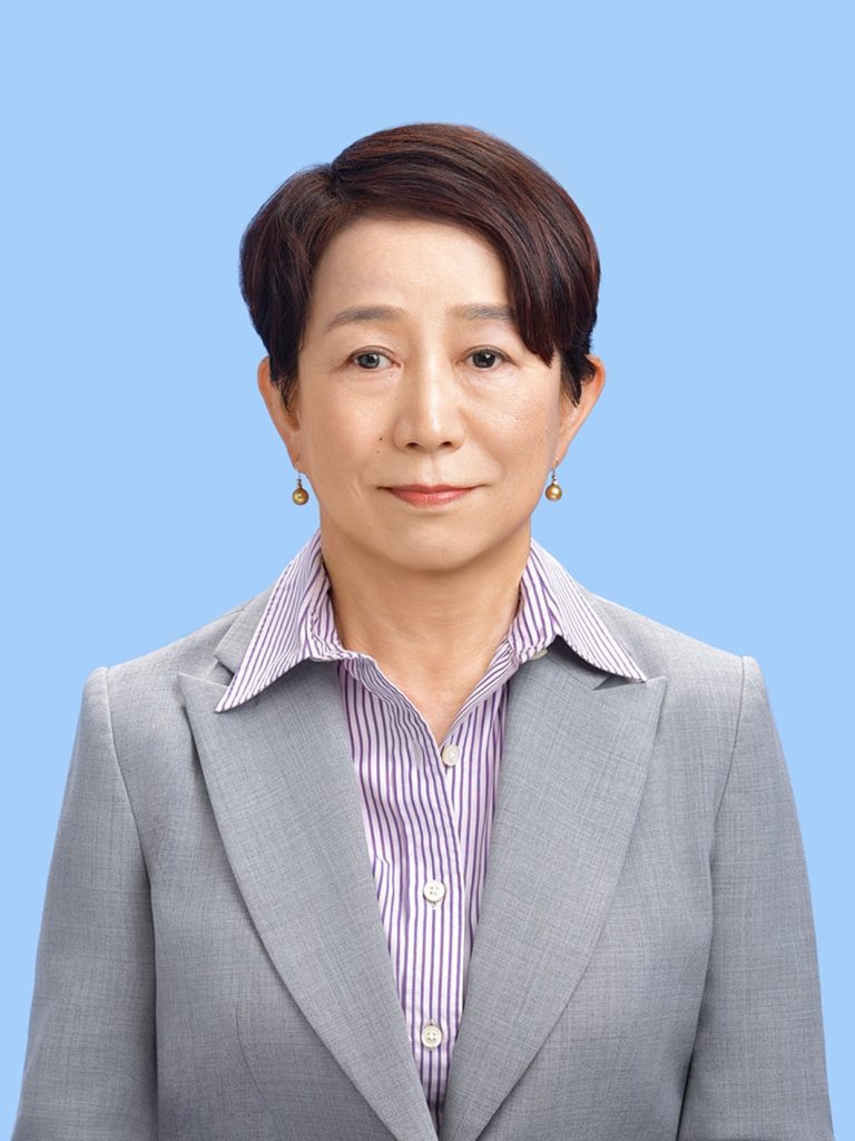
Factory Integration (FI) - Supika Mashiro, TEL
Abstract
Factory Integration includes everything that is needed to keep semiconductor manufacturing operation in the Fab undisrupted at affordable cost and in sustainable manner. Its planned focus areas in coming version, such as Digital Twin interoperability in fab and beyond, smart manufacturing advancement through adoption of robotics, and security aspects of semiconductor manufacturing operations, will be discussed in this presentation.
Bio - Supika Mashiro
Supika Mashiro works as an Advisor for Tokyo Electron Limited at its HQ in Tokyo, Japan. She has been involved in Factory Integration (FI) IFT of IRDS since its inauguration in 2016 and a cochair since 2017. Her area of interest and involvement encompasses smart manufacturing as well as environment and safty/ Sustainability road-mapping and related industry standard development.
- 12:10–12:40
Metrology (MET) - Carlos Beitia, CEA
Abstract
Today industry trend is application driven by system architecture solutions. This was one of the transformative reasons from the old ITRS process-device-technology centered roadmap toward IRDS System and Device centered. This transformation of the industry cannot be done without yield and high-volume manufacturing solution. Metrology need to embrace the new paradigm and transform itself from a material and process centered control tool to at most holistic innovation and acceleration one. Consequently, from the holistic approach, metrology will need to consider Material to System Technology Co Optimization MSCO needs and cross domain data and knowledge exchange to support this approach. In the methodology and tools aspects metrology need to integrate IA to break knowledge and data silos in the FAB to accelerate yield learning. Finally at the material and process level metrology will need to track traditional issues from Material/Process perspective but will need to include System/application metrology data that can add constraints or degree of freedom for the MSCO approach.
Bio - Carlos Beitia
More than 25 years in semiconductor from Research, R&D up to Industrial application. September 2022-now, Key Account Manager CEA-Leti, Materials Program Line Manager and Metrology Expert for the Technological Research Division. 2020-2022 Vice President Strategic Alliance at Unity-Semiconductor, 2029 Vice President R&D Unity Semiconductor. From 2009-2019 at Leti, work at different positions in metrology activities (Metrology R&D business development, Metrology Silicon Platform Division Deputy Manager, Scientific Manager of In-line Metrology Laboratory). Previously Application Engineer for 8 years with KLA-Tencor from junior to senior worldwide support.
14:50 - 15:15 | Thermoelectric energy harvesting and cooling technology; New developments - Takao Mori, NIMS:
Abstract
Thermoelectric materials can be used for various energy harvesting power generation applications, or solid-state cooling. We have been utilizing novel routes such as magnetism, Anderson localization, defect engineering, etc. to overcome traditional physical properties tradeoffs and achieve high thermoelectric performance. As a result, we have succeeded in developing novel materials & modules that surpass the half-century champion Bi2Te3-type. Electrode technologies for these new materials were also developed, with a novel concept of “active electrodes” leading to high stability and enhancement of the device performance, also for diffusion barrier materials. Effective methodology for designing high performance thermoelectric modules (TEGs) has also been developed. Accurate evaluation of performance of actual devices is critical for industrialization, and we have also laid out the best practices for evaluation of TEGs. We also made advancements in fabrication of various formats of TEGs: bulk, thin film, flexible. Thermal management technologies are also being developed. Cooling is becoming increasingly critical for data centers and the semiconductor industry, and we have also fabricated Peltier devices of novel materials, together with developing viable active cooling materials to realise the next generation cooling. Support from JST Mirai Large-Scale Program JPMJMI19A1 is acknowledged.
Bio - Takao Mori
Takao Mori received his PhD at U. Tokyo, Dept. Physics. He is a Field Director at National Institute for Materials Science (NIMS) and Professor of U. Tsukuba Graduate School, and elected Board Member, present President of the International Thermoelectric Society (ITS). Mori’s research interests are, broadly speaking, to find ways to control structures and properties of inorganic materials. He is especially involved in development of thermoelectric materials and multidisciplinary enhancement principles, such as utilizing magnetism, in order to find new routes to achieve high control over band structures and electrical and thermal transport. And furthermore, working on thermoelectric devices, module and thermal management technology for applications. Mori is a Senior Editor of Materials Today Physics, Advisory Board Member of JSSC, J. Materiomics, PRX Energy, Joule, Device. He is a Program Manager of JST Mirai Large-scale Program. Mori has published over 500 papers, 25 book chapters, 40 patents.
15:15 - 15:40 | Tailoring the Physical Properties of Narrow-Gap Semiconductor Mg2S Thermoelectric Thin Films through Defect Engineering - Takeaki Sakurai, University of Tsukuba
Abstract
Thin-film-based miniature thermoelectric (TE) devices are attracting attention for Internet of Things (IoT) applications because they can effectively recover waste heat generated within electronic components. Among various thermoelectric materials, Mg2Sn and related Mg2(Sn,Ge) compounds are considered promising low-cost candidates that perform well in the temperature range near room temperature. This study explores the enhancement of thermoelectric properties in p-type Mg2Sn-based epitaxial thin films through defect engineering and doping strategies. By optimizing the synthesis process and precisely incorporating dopants, significant improvements in both electrical and thermoelectric performance were achieved. The control of defect structures with Ge incorporation and Mg flux modulation, such as vacancies and stacking faults, played a crucial role in modulating phonon scattering and charge transport, leading to enhanced thermoelectric efficiency. Doping strategies, particularly the introduction of Li for p-type conductivity, proved essential in balancing electrical conductivity and the Seebeck coefficient. These findings underscore the importance of combining precise doping control and defect management to develop high-performance thermoelectric materials. This work hopes to provide valuable insights for advancing the design and optimization of Mg2Sn-based systems, making them more suitable for next-generation energy-harvesting applications.
Bio - Atsushi Ogura
Dr. Takeaki Sakurai is an Executive Officer and Professor at University of Tsukuba, Japan. His research focuses on compound semiconductor materials and their application to high-efficiency solar, thermal, and chemical energy conversion devices. He also oversees the coordination of international collaborative projects in his executive role.
- 12:40–13:10
Lithography and Patterning - Mark Neisser, Tsingha University
Abstract
The IRDS 2025 lithography and Patterning roadmap has recently been published. High NA exposure tools are in full use in chip process development and are expected to be used in production as early as next year. They provide better resolution and simpler processes for upcoming logic products but also have a smaller field size. Key challenges are stochastics, process control, overlay, small field sizes and cost. Addressing these challenges will require improved masks, higher power light sources, improved resists and many process improvements. The requirements for better interchip connections are expected to drive improved packaging lithography. After 0.55NA lithography, hyper NA EUV with an NA in the range of 0.75 may be implemented if it is cost effective as a replacement for 0.55NA EUV with multiple patterning. Research efforts on shorter wavelengths than EUV are underway, but so far there is no consensus or feasibility demonstration on any of the several wavelengths under consideration. Nor are there device structures in the current IRDS roadmaps that clearly need the capabilities of a shorter wavelength. Device structures are becoming more three dimensional, with some circuit elements moving to the back of the chip. This creates challenges in overlay and patterning, but slows down the rate of scaling on the front of the chip.
Bio - Mark Neisser
Mark Neisser is a chair professor in the School of Integrated Circuits at Tsinghua University. He is also the Director of the Photoresist lab at the Integrated Circuit Research Platform at the International Innovation Center of Tsinghua University, Shanghai. He received his B.S. degree in chemistry from Cornell University and his M.S. and Ph.D. degrees in chemistry from the University of Michigan. He is the author of more than 30 US patents, over 100 journal papers and has co-authored two book chapters. He is the chairman of the IRDS roadmap committee for lithography and patterning. Dr. Neisser worked at IBM doing semiconductor lithography research, followed by positions managing research and development of photoresists and of ancillary materials for lithography. His current research interests involve EUV resists, semiconductor patterning and related materials, and the physics of imaging or patterning such materials.

14:50 - 15:15 | Thermoelectric energy harvesting and cooling technology; New developments - Takao Mori, NIMS:
Abstract
Thermoelectric materials can be used for various energy harvesting power generation applications, or solid-state cooling. We have been utilizing novel routes such as magnetism, Anderson localization, defect engineering, etc. to overcome traditional physical properties tradeoffs and achieve high thermoelectric performance. As a result, we have succeeded in developing novel materials & modules that surpass the half-century champion Bi2Te3-type. Electrode technologies for these new materials were also developed, with a novel concept of “active electrodes” leading to high stability and enhancement of the device performance, also for diffusion barrier materials. Effective methodology for designing high performance thermoelectric modules (TEGs) has also been developed. Accurate evaluation of performance of actual devices is critical for industrialization, and we have also laid out the best practices for evaluation of TEGs. We also made advancements in fabrication of various formats of TEGs: bulk, thin film, flexible. Thermal management technologies are also being developed. Cooling is becoming increasingly critical for data centers and the semiconductor industry, and we have also fabricated Peltier devices of novel materials, together with developing viable active cooling materials to realise the next generation cooling. Support from JST Mirai Large-Scale Program JPMJMI19A1 is acknowledged.
Bio - Takao Mori
Takao Mori received his PhD at U. Tokyo, Dept. Physics. He is a Field Director at National Institute for Materials Science (NIMS) and Professor of U. Tsukuba Graduate School, and elected Board Member, present President of the International Thermoelectric Society (ITS). Mori’s research interests are, broadly speaking, to find ways to control structures and properties of inorganic materials. He is especially involved in development of thermoelectric materials and multidisciplinary enhancement principles, such as utilizing magnetism, in order to find new routes to achieve high control over band structures and electrical and thermal transport. And furthermore, working on thermoelectric devices, module and thermal management technology for applications. Mori is a Senior Editor of Materials Today Physics, Advisory Board Member of JSSC, J. Materiomics, PRX Energy, Joule, Device. He is a Program Manager of JST Mirai Large-scale Program. Mori has published over 500 papers, 25 book chapters, 40 patents.
15:15 - 15:40 | Tailoring the Physical Properties of Narrow-Gap Semiconductor Mg2S Thermoelectric Thin Films through Defect Engineering - Takeaki Sakurai, University of Tsukuba
Abstract
Thin-film-based miniature thermoelectric (TE) devices are attracting attention for Internet of Things (IoT) applications because they can effectively recover waste heat generated within electronic components. Among various thermoelectric materials, Mg2Sn and related Mg2(Sn,Ge) compounds are considered promising low-cost candidates that perform well in the temperature range near room temperature. This study explores the enhancement of thermoelectric properties in p-type Mg2Sn-based epitaxial thin films through defect engineering and doping strategies. By optimizing the synthesis process and precisely incorporating dopants, significant improvements in both electrical and thermoelectric performance were achieved. The control of defect structures with Ge incorporation and Mg flux modulation, such as vacancies and stacking faults, played a crucial role in modulating phonon scattering and charge transport, leading to enhanced thermoelectric efficiency. Doping strategies, particularly the introduction of Li for p-type conductivity, proved essential in balancing electrical conductivity and the Seebeck coefficient. These findings underscore the importance of combining precise doping control and defect management to develop high-performance thermoelectric materials. This work hopes to provide valuable insights for advancing the design and optimization of Mg2Sn-based systems, making them more suitable for next-generation energy-harvesting applications.
Bio - Atsushi Ogura
Dr. Takeaki Sakurai is an Executive Officer and Professor at University of Tsukuba, Japan. His research focuses on compound semiconductor materials and their application to high-efficiency solar, thermal, and chemical energy conversion devices. He also oversees the coordination of international collaborative projects in his executive role.
Lunch
- 14:30-15:00
More than Moore (MtM) – Alan O'Riordan, Tyndall National Institute
Abstract
Bio - Alan O'Riordan
Prof Alan O’Riordan is Head of the Precision Electrochemical Nanosensor Research Group, comprising support and research staff, postdoctoral researchers, and PhD students. The Group is developing nanoelectrochemical sensor technologies on silicon chip substrates, providing highly sensitive, selective, and reliable measurements. Their work is focused on smart sensors and systems for sustainable agri-food and environmental applications. He is a Principal Investigator in the Research Ireland Research Centre Vistamilk and leads the IEEE International Focus Team on More-than-Moore, part of the IEEE International Roadmap for Devices and Systems.
He has competitively secured, as Principal Investigator, national and EU research projects worth approximately €17 million in total research funding. He has published over 100 peer-reviewed publications and holds one granted patent, Nanowire Electrode Sensor (EU & US – US 20140145709), with another pending. He has twice been awarded the Enterprise Ireland Gold Medal for Most Innovative Technology Emerging from Third Level.
Prof O’Riordan is a Steering Committee member of the Royal Society of Chemistry – Electroanalytical Sensors and Systems Group, and is also a member of the IEEE. He holds an adjunct research professorship at the Indian Institute of Technology, Hyderabad.
He received his BSc in Analytical Chemistry in 1995 and a PhD in Chemistry (Nanotechnology) in 2005. To date, he has graduated 17 PhD and 3 MSc students.
- 15:00-15:30
More Moore (MM) - Mustafa Badaroglu, Qualcomm
Abstract
Bio - Mustafa Badaroglu
- 15:30-16:00
Packaging Integration (PI) - Dev Gupta, APSTL
Abstract
Bio - Mustafa Badaroglu
- 16:00-16:30
Beyond CMOS & Emerging Materials (BC & EMI) -
Abstract
Bio
Next Steps and Closing Remarks - Paolo Gargini
Day 2 : 19 May
- 08:30-11:00
Tutorial - New Materials for Electronics
08:30 - 11:55 | Neuromorphic computing based on 2D materials - Andrea Capasso, INL
09:00 - 09:30 | New memory devices based on emerging materials - Hanwool Yeon, Gwangju Institute of Science and Technology
09:30 - 10:00 | Emerging materials for computation compatible with CMOS - Satarship Das, Penn State University
10:00 - 10:30 | 2D Materials for computation - Xinran Wan, Nanjing University
10:30 - 11:00 | More-than-Moore applications based on 2D materials - Francisco Gamiz, UGR & FAMES Pilot Line
- 11:45-13:00
New Directions in Computing
11:45 - 12:35 | Spiking Manifesto - Eugene Izhikevich, SpikeCore
Abstract
Modern AI models have increasingly larger dimensions to maximize their representational capacity, requiring GPUs to perform multiplications of huge matrices. In contrast, the brain’s spiking neural networks exhibit factorially explosive encoding capacity even when their size is small. This manifesto proposes a framework for thinking about popular AI models in terms of spiking networks and polychronization, and for interpreting spiking activity as nature’s way of implementing look-up tables. This suggests a path toward converting AI models into a novel class of architectures with much smaller size yet combinatorially large representation capacity, offering the promise of a thousandfold improvement in performance
Bio - Eugene Izhikevich
Eugene Izhikevich is the founder and CEO of SpikeCore in San Diego, the founder and Chairman of the Board of Brain Corp, and the founder and Editor‑in‑Chief of Scholarpedia, the peer‑reviewed encyclopedia.
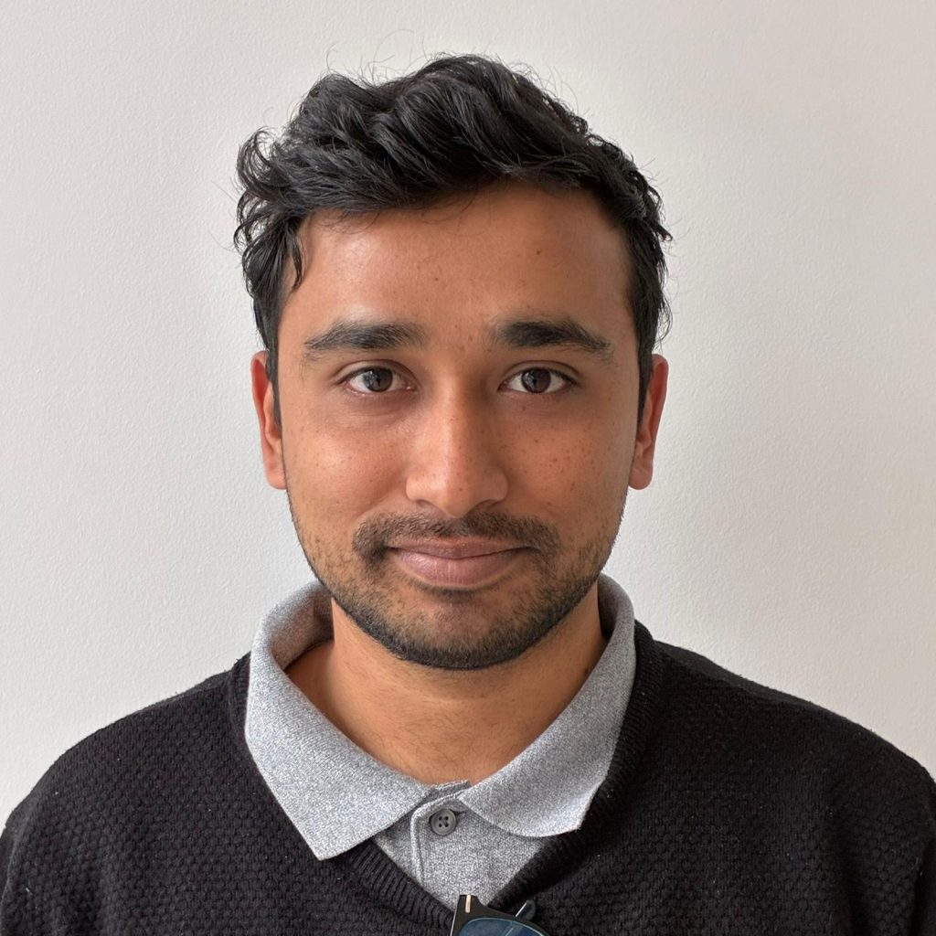
12:35 - 13:00 | A Hybrid Memristor-Magnetic Tunnel Junction Ising Machine - Mohammed-akib Iftakher
Abstract
Hardware Ising machines offer a path to solving large-scale optimization tasks. We present an integrated Ising machine combining two nanotechnologies: memristor crossbars for multi-level coupling weights and stochastic magnetic tunnel junctions (SMTJs) as thermally driven spins. By utilizing identical read voltage to access the crossbar and bias the SMTJs, we demonstrate an intrinsic, analog-native annealing technique. Our CMOS-compatible prototype, operating at zero magnetic field, consistently finds global optima for weighted MAX-CUT and graph-coloring problems. This co-integrated approach provides a scalable, energy-efficient pathway for 3D-integrated Ising solvers.
Bio - Mohammed Akib Iftakher
Mohammed Akib Iftakher is a senior PhD candidate at the University of Paris-Saclay/CNRS, specializing in emerging memory technologies and analog IC design. He holds an M.Sc. in Integrated Circuit System from the University of Paris-Saclay and a B.Eng. in Electrical Engineering from the University of Malaya. His recent research on hybrid memristor-MTJ Ising machines is currently under review at Nature Communications. He is currently focused on developing CMOS-integrated, physics-inspired learning mechanisms for high-performance computing.
- 14:30-18:30
New Directions in Materials and Devices for Computing
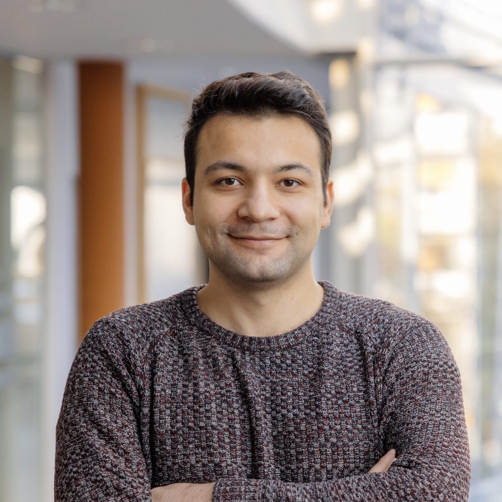
14:30 - 15:05 | The Dirac-Source FET and the neverending quest for steep-slope switches - Luca Selmi, University of Modena & IUNET
Abstract
The quest for reduced switching energy in digital circuits is increasingly limited by the Boltzmann tyranny, which prescribes a minimum subthreshold swing of 60 mV/dec for thermionic emission devices. Numerous steep slope transistor concepts have been proposed in the attempt to beat this limit, none of which has yet made it to mainstream technologies. In this context, we aim to present recent results on the Dirac-Source Field Effect Transistor, a recently proposed steep slope FET exploiting the unique properties of Dirac-material / Semiconductor junctions.
Bio - Luca Selmi
Luca Selmi (PhD 1992, Fellow IEEE 2015) is Professor of Electronics at Università degli Studi di Modena e Reggio Emilia. His research interests cover modeling, simulation, and characterization of micro/nanoelectronic devices for switching and sensing. They led him to co-author more than 350 peer-reviewed publications, book chapters and a Cambridge University Press book on Nanoscale MOS Transistors. He has served as IEEE EDL associate editor, as TPC member of IEEE IEDM, VLSI Symposium, ESSDERC and as chair of numerous international conferences and events in the area of electron devices. From 2017 to 2022 he directed the IUNET consortium on nanoelectronics and he currently coordinates the EU Chips-JU project “AttoSwitch”.
15:05 - 15:40 | Ferroelectrically switchable quantum geometry for in-memory computing - Peng Song, NTU
Abstract
Most existing implementations of low-power electronic devices rely on the classical charge degree of freedom of electrons as the information carrier. Identifying the quantum characteristics of electrons as a new information carrier can provide a promising pathway to realize low-power electronics with functionality and performance far beyond traditional electronics. Quantum geometry—the intrinsic geometric structure of Bloch wavefunctions in momentum space—offers a compelling physical platform to address this challenge. In this talk, I will discuss our recent efforts of exploring quantum geometry in quantum materials, including its transport manifestation, non-volatile switching1, and finally the possibility of implementing a novel in-memory computing2.
Bio - Peng Song
Peng Song received his Bachelor degree in 2012 at Fudan University, and PhD degree in 2016 at National University of Singapore (NUS). From 2017 to 2021, he continued his postdoc research at NUS and then at Max Planck Institute of Microstructure Physics. His research in two-dimensional materials physics and electronic devices has led to several major breakthroughs in spin-orbit physics and publications in top scientific journals (Nature, Nature Materials etc). In May 2021, he was awarded the prestigious Nanyang Assistant Professorship and joined School of Electrical & Electronic Engineering, Nanyang Technological University (NTU) as an Assistant Professor. At NTU, he is interested in exploring novel device physics in low-dimensional materials and topological quantum materials, and their further integration into novel computing devices and architectures.
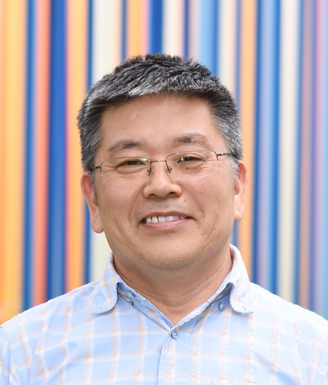
15:40 - 16:05 | Silicon devices for cryogenic computing - Qing-Tai Zhao, FZJ
Abstract
High-performance computing based on von Neumann architecture suffers from high power consumption at room temperature. Cryogenic computing, including von Neumann, neuromorphic and quantum systems, offers a way forward for highly energy-efficient big data processing. CMOS technology is central to this development, but it must operate at ultra-low power under cryogenic conditions. However, conventional CMOS, which is designed for room temperature, faces significant challenges at temperatures close to absolute zero. These include an increased subthreshold swing (SS) caused by band-tail effects, as well as an elevated threshold voltage resulting from bandgap widening and Fermi-level shifts. Addressing these issues is therefore critical. This presentation will discuss these challenges and the prospects for cryogenic CMOS. The use of a single transistor based on FDSOI FET for cryogenic memory will also be addressed.
Bio - Qing-Tai Zhao
Qing-Tai Zhao completed his PhD in physics at Peking University. He then joined the Institute of Microelectronics at Peking University as lecturer and associate professor, where he focused on the research of SOI materials and devices. In 1997, he was awarded a Humboldt Research Fellowship, which led him to Forschungszentrum Jülich in Germany, where he currently leads a research group specializing in nanoelectronic devices. His primary research interests include Si-Ge-Sn based high mobility devices and technology, FDSOI and nanowire devices for low power applications, as well as ferroelectric-based neuromorphic devices and cryogenic electronics for quantum computing. He has authored and co-authored around 300 peer-reviewed publications and holds over 40 patents.
16:45 - 17:20 | Toward fab-compatible processing of 2D materials to neuromorphic devices - Burkay Uzlu, AMO
Abstract
Two-dimensional materials offer unique opportunities for next-generation applications due to their atomic thickness, electrostatic tunability, and compatibility with heterogeneous integration. In this talk, I will discuss progress toward fab-compatible wafer-scale processing of 2D materials and their integration into CMOS platforms. Key challenges such as variability, interface engineering, and scalable process modules will be highlighted. I will further present recent demonstrations of nanoscale memristive devices based on 2D materials and their integration onto silicon microchips, enabling low-voltage switching and potential applications in neuromorphic computing architectures.
Bio - Burkay Uzlu
Burkay Uzlu received his B.S. and M.S. degrees in Physics from Bilkent University, Turkey, and his Ph.D. in Electrical Engineering from RWTH Aachen University, Germany. He was a postdoctoral researcher at Northwestern University before joining AMO GmbH, where he currently works as a Research Associate. His research focuses on the development and scalable integration of two-dimensional (2D) materials for next-generation electronic and optoelectronic devices. His work includes wafer-scale fabrication, CMOS-compatible integration, and novel device concepts such as Dirac field-effect transistors (Dirac FETs) and memristive devices for emerging computing architectures.
17:20 - 17:55| Embodied AI: When Intelligence Emerges from Hardware - Adrian Ionescu, EPFL
Abstract
Embodied Artificial Intelligence represents a paradigm shift in which intelligence emerges from the tight integration of sensing, actuation, computation, and learning within physical systems. Rather than treating AI as a purely algorithmic layer, embodied AI emphasizes the co-design of hardware, materials, and algorithms to enable adaptive, energy-efficient and context-aware behavior at the edge. This talk will introduce the core concepts of embodied AI and discuss the electronic technologies that enable it, including advanced sensors, bio-integrated and neuromorphic devices, in-memory and ferroelectric computing, and ultra-low-power edge architectures. Examples covering robotics, wearables and cyber-physical systems will illustrate how hardware–software co-design unlocks new capabilities beyond conventional AI platforms.
Bio - Adrian Ionescu
Adrian Ionescu is Full Professor of Nanoelectronics at EPFL and Director of the Nanoelectronic Devices Laboratory. His research focuses on advanced semiconductor devices, energy-efficient and neuromorphic electronics, bio-integrated sensors and hardware foundations for edge and embodied AI. He has authored more than 500 scientific publications and is the recipient of multiple ERC grants, IEEE awards, and international distinctions. Prof. Ionescu is actively involved in large-scale European and international initiatives at the intersection of AI, quantum electronics, nanoelectronics and health technologies, and is a founder or scientific advisor to several deep-tech startups. He currently serves in senior academic leadership roles at EPFL, where he contributes to strategic programs in engineering.
17:55 - 18:30 | Nonlinear Multimode NEMS for Energy-efficient Temporal Computing - Selim Hanay, INL
Abstract
As CMOS scaling approaches physical and energy-efficiency limits, alternative device concepts are being explored to enhance system-level computing performance. Nanoelectromechanical systems (NEMS) resonators provide intrinsic nonlinearity at ultra-low power, high quality factors, and compact footprints. In multimode NEMS devices, strong intra- and inter-modal coupling generates rich, high-dimensional dynamics, while long ring-down times enable short-term memory. These properties make NEMS attractive for physical reservoir computing and temporal signal processing. This talk presents experimental demonstrations of nonlinear multimode NEMS for time-series analysis and discusses their potential relevance to emerging heterogeneous and beyond-CMOS computing paradigms highlighted in IRDS roadmaps.
Bio - Selim Hanay
Selim Hanay is a Research Group Leader at INL – International Iberian Nanotechnology Laboratory. He received his B.Sc. in Microelectronics Engineering from Sabancı University and his Ph.D. in Physics from Caltech in 2011, where he developed NEMS-based single-molecule sensors. In 2013, he joined the faculty of Bilkent University, pioneering nonlinear NEMS and microwave resonator platforms for sensing and information processing. In 2025, he joined INL to advance NEMS-based computing architectures. He is the recipient of multiple national research awards and European Research Council (ERC) Starting and Proof-of-Concept grants.
- Agenda
Other events
Workshops, conferences and meetings of the JASMINE network
2nd EU-Japan Digital Foundations Network Symposium
May 18
Upon registration
- Workshop
2026 IRDS/ISRDS Workshops
IRDS – Annual Update of Roadmap Summaries
- Granada, Spain
- 100+ participants
Mar 24
Upon registration
- Workshop
Japan-EU Cooperation on Advanced Computing & Functionalities, Heterogeneous Integration and Semiconductor Value Chain
2nd EU-JAPAN DIGITAL WEEK 2026
- School of Engineering, University of Tokyo, Japan
- 200+ participants
Our partners
INPACE Hub
About this partner
INPACE’s mission is to support the implementation of the Digital Partnerships between the European Union and Japan, South Korea, Singapore, as well as the Trade and Technology Council with India.
Powered by a consortium of 21 European and Asian partners, the initiative establishes a multi-stakeholder Hub for collaboration in digital technologies between Europe and the Indo-Pacific region and fosters long-term cooperation in key digital technologies by bringing together experts and stakeholders from both regions.
- Association
SiNANO Institute
🇫🇷 France
About this partner
The SINANO Institute is the European Academic and Scientific Association for Nanoelectronics, acting as a network of excellence connecting the European Research and Academic community in semiconductor science and technologies. It gathers 27 academic/RTO members and 22 deep-tech start-ups in the area of fabrication, characterization, modelling, design and simulation of emerging nanoelectronic materials, devices, circuits and systems from 16 European Countries. The SiNANO mission is to secure the future of European semiconductor science and technology by mobilizing and nurturing the European R&I community, promoting and strengthening synergies in the field through our membership, accelerating the translation of excellent research into European knowhow, technologies, and products, ensuring the pipeline of talented researchers and the growth of skilful talent in an inclusive and diverse. SiNANO is the European representative of IRDS “International Roadmap for Devices and Systems.