2nd EU-JAPAN DIGITAL WEEK 2026
in Tokyo on 24-25 March 2026!
The workshop will focus on key areas of the INPACE Cluster dedicated to “Enabling technologies – Chips for the future” and is aligned with the topics defined in the Digital Partnerships between EU and Japan. The presentations and discussions will cover the many semiconductor challenges (complex value chain, computing and storage needs, novel functionalities for electronic systems, circuit and system integration, energy & material needs, reliability) and possible technological solutions, especially: reductions of energy and material consumption for sustainable electronic systems, advanced logic devices and materials, integration of novel functionalities for future electronic systems (e.g. smart sensing, energy harvesting for autonomous system, power devices, photonics, cryoelectronics for quantum engineering), heterogeneous 3D integration and packaging for high performance, low power, low latency, miniaturisation, integration of new functionalities and lower cost of electronic systems, and possible cooperation on gaps in the semiconductor value chain.
This workshop is associated with the newly launched “Japan and EU Semiconductors: Mutual Innovation & Excellence” JASMINE Project.
Hongo University of Tokyo – Haseko Kuma Hall

Programme
Day 1 : 24 March
- 9:00-9:10
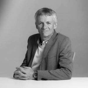
Opening remarks - Francis Balestra
Bio
Francis Balestra
BALESTRA Francis, CNRS Research Director at CROMA, is Director Emeritus of the European SiNANO Institute and Chair of IEEE Electron Device Society France, and has been Director of several Research labs. He coordinated many European Projects (ICOS, NEREID, NANOFUNCTION, NANOSIL, etc.) that have represented unprecedented collaborations in Europe in the field of Nanoelectronics. He founded and/or organized over 50 international Conferences and Workshops, and has co-authored more than 500 publications. He is member of several European Scientific Councils, of the Advisory Committees of International Journals and of the IRDS (International Roadmap for Devices and Systems) International Roadmap Committee as representative of Europe.
- 9:10-10:25
Session 1 – Smart Sensors
9:10 - 9:35 | Smart Sensors - Alan O’Riordan, Tyndall National Institute
Abstract
With the global population expected to grow to over 9.6 billion by 2050 it is a projected that a 50-60 % increase in food production will be required. A key challenge then, going forward, will be to sustainably close the food gap. This must be achieved against the backdrop of climate change & desertification, labour shortages and competition for energy, land & resources. It is clear then, that addressing this challenge will require the development of more efficient and sustainable food production techniques and processes. To this end, new digital technologies, that are fit for purpose, are urgently required to digitise the entire food chain. This convergence between the Internet of Things (IoT) and the agri-food industry requires sensor systems and technologies that provide real time data to producers and processers; required for rapid, but informed, decision making. This talk will provide an overview on current problems in agriculture and demonstrate application of different biosensor developed within our group to address the sustainability issues currently being experienced in this sector.
Bio - Alan O'Riordan
Prof Alan O’Riordan is Head of the Precision Electrochemical Nanosensor Research Group, comprising support and research staff, postdoctoral researchers, and PhD students. The Group is developing nanoelectrochemical sensor technologies on silicon chip substrates, providing highly sensitive, selective, and reliable measurements. Their work is focused on smart sensors and systems for sustainable agri-food and environmental applications. He is a Principal Investigator in the Research Ireland Research Centre Vistamilk and leads the IEEE International Focus Team on More-than-Moore, part of the IEEE International Roadmap for Devices and Systems.
He has competitively secured, as Principal Investigator, national and EU research projects worth approximately €17 million in total research funding. He has published over 100 peer-reviewed publications and holds one granted patent, Nanowire Electrode Sensor (EU & US – US 20140145709), with another pending. He has twice been awarded the Enterprise Ireland Gold Medal for Most Innovative Technology Emerging from Third Level.
Prof O’Riordan is a Steering Committee member of the Royal Society of Chemistry – Electroanalytical Sensors and Systems Group, and is also a member of the IEEE. He holds an adjunct research professorship at the Indian Institute of Technology, Hyderabad.
He received his BSc in Analytical Chemistry in 1995 and a PhD in Chemistry (Nanotechnology) in 2005. To date, he has graduated 17 PhD and 3 MSc students.
9:35 - 10:00 | Genki Yoshikawa – NIMS
Abstract
Olfactory sensors (electronic nose, e-nose) are the last frontier of the five senses. They are expected to contribute to applications where other sensors are difficult to access, such as metabolism, where invisible chemical reactions are major targets. For practical artificial olfaction, we developed a Membrane-type Surface stress Sensor (MSS) based on microelectromechanical systems (MEMS) technologies. MSS offers various practical features, including high sensitivity, small size, chemical diversity, room-temperature operation, mechanical/electrical stability, low power consumption, and rapid response. On this unique platform, research and development on both hardware and software are ongoing, including the development of various functional receptor materials and the integration with machine learning. Furthermore, the MSS Alliance/Forum/Partnership, one of the world’s largest industry-academia-government collaboration schemes in olfactory sensors, has been organized, accumulating a vast amount of know-how. Currently, various field trials have been conducted, particularly for biological gas measurements in agricultural and medical applications, as well as by a newly launched NIMS startup company (Qception Corporation).
Bio - Genki Yoshikawa
Genki Yoshikawa is Group Leader of the Olfactory Sensors Group at the National Institute for Materials Science (NIMS), Japan, Professor at the University of Tsukuba, and Chief Technical Officer (CTO) of Qception Corporation. He received the B.S. (1999), M.S. (2001), and Ph.D. (2004) degrees in Science from the University of Tokyo. He previously served as Assistant Professor at Tohoku University (2005–2008), Visiting Scientist at the University of Basel (2007–2009), ICYS-MANA Researcher (2009–2011), and Independent Scientist at NIMS (2011–2016).
He has authored 100+ peer-reviewed publications, holds 30+ domestic and international patents, and has delivered 200+ invited and keynote lectures. He has led 10+ competitively funded projects, including PRISM and JST-CREST, and has received 10+ awards; his work has been featured in 100+ newspaper articles and TV reports.
He is the inventor of the Membrane-type Surface stress Sensor (MSS), which has been commercialized as an optimized nanomechanical sensor platform. He also led one of the world’s largest industry–academia–government consortia in olfactory sensing (MSS Alliance/Forum/Partnership), involving 50+ companies, universities, research institutes, and hospitals. His research is dedicated to developing practical olfactory sensing systems by integrating hardware (sensing elements, receptor materials, and system optimization), software (multivariate analysis and machine learning), and fundamental science (analytical modeling, fluid dynamics, and surface science) toward world peace.
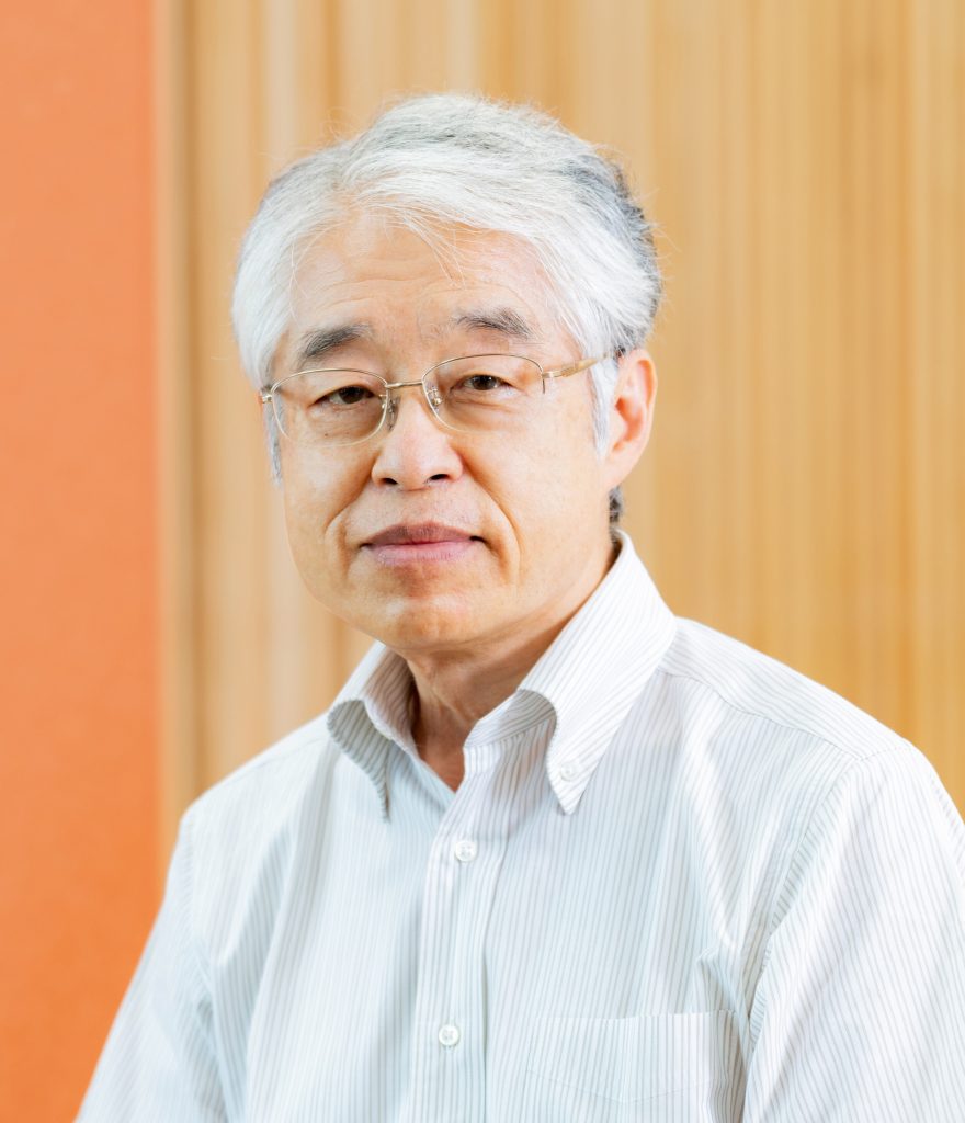
10:00 - 10:25 | Molecular Sensors for Smart Society - Ken Uchida, University of Tokyo
Abstract
The rapid aging of the global population is a significant social challenge. As the elderly population grows, more and more people will need continuous medical care. However, the number of hospitals and medical facilities is finite, making it increasingly challenging to treat or provide long-term care for all patients who need it. Therefore, home-based healthcare and monitoring will be an integral part of the future medical system. It could provide adequate monitoring of patients’ health conditions and chemical environments to ensure safe home care during the ongoing pandemic. One strategy to accomplish this is to use molecular sensors to detect low concentrations of gases in living environments. These sensors continuously measure molecules related to human metabolism and the environment, offering helpful information about health status and possible daily life risks.
This presentation will introduce our recent advances in molecular sensing technologies for healthcare monitoring. Special attention will be given to sensing strategies that detect hydrogen, hydrogen sulfide, and other molecular species in human breath. These gases are potential key biomarkers for physiological conditions and disease states. The principles of sensor operation will be also discussed.
Bio - Atsushi Ogura
Ken Uchida received the B.S. degree in Physics, M.S. and Ph.D. degrees in Applied Physics from The University of Tokyo, Japan, in 1993, 1995 and 2002, respectively. In 1995, he joined the R&D Center of Toshiba Corporation. In 2008, he moved to Tokyo Institute of Technology as an associate professor. In 2012, he moved to Keio University, as a full professor, and then to the University of Tokyo, as a full professor. He has studied the physics of nanoscale devices.
10:25 – 10:45 | Coffee break
- 10:25-12:00
Session 2 – Process Technology & Manufacturing & Sustainability
10:45 – 11:10 | The Future of Compute: From Atomic-Scale Scaling to System-Level Integration - Nadine Collaert, imec
Abstract
The AI-driven compute explosion is necessitating a shift from traditional scaling to a holistic, system-level approach. To extend logic beyond current limits, nanosheet transistors and CFETs are being integrated with advanced power delivery and 3D stacking. As monolithic scaling reaches its physical boundaries, heterogeneous integration and chiplet-based architectures are essential for sustaining performance. Managing escalating power densities through energy-aware design and advanced thermal solutions is now a primary requirement. Concurrently, in-memory computing, neuromorphic architectures, and early quantum platforms are emerging to provide high-efficiency, data-centric alternatives to the classical paradigm, defining the next generation of advanced computing.
Bio - Nadine Collaert
Nadine Collaert is an imec fellow and part-time professor at VUB (Brussels, Belgium). She is currently leading the technology office in the connected computing sector, focusing on identifying cutting-edge advancements in wireless, wireline, optical communications, and emerging computing technologies to drive future innovation. Before that, she was responsible for the advanced RF program looking at heterogeneous integration of III-V/III-N devices with advanced CMOS to tackle the challenges of next generation mobile communication. Before that, she was program director of the LOGIC Beyond Si program focused on the research on novel CMOS devices and new material-enabled device and system approaches to increase functionality. She has been involved in the theory, design, and technology of FinFET devices, emerging memories, transducers for biomedical applications and the integration and characterization of biocompatible materials. She has a PhD in electrical engineering from KU Leuven and she holds more than 500 publications and more than 15 patents in the field of device design and process technology
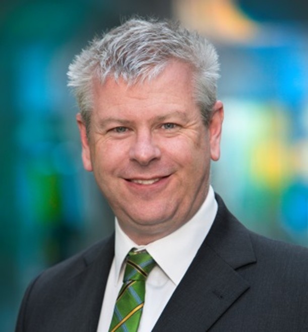
11:10 – 11:35 | The necessary transformation to secure a sustainable semiconductor industry - Laurent Pain, CEA-LETI
Abstract
The semiconductor industry is central to the global digital transition, with rapid growth driven by artificial intelligence, 5G, and cloud computing. Through its Chip Act initiative, the European Union aims to increase its global manufacturing capacity by 2030, but this expansion poses significant environmental challenges. Semiconductor production is highly resource-intensive, consuming large amounts of energy, water, critical materials, and generating complex waste, including rising electronic waste and data-center emissions. Addressing these impacts requires systemic transformation through responsible manufacturing, efficient technologies, eco-design, circularity, and algorithmic sobriety. This talk will examine how to integrate the principles of sustainable development into the semiconductor industry to ensure its long-term economic and environmental viability.
Bio - Laurent Pain
Laurent Pain is graduated from Grenoble INP – PHELMA engineering school in 1992. He received his Ph D after his work on DUV resists study. He joined CEA-Leti in 1996 to work on infra-red technology, and then moved to STmicroelectronics in 1999 working on 193nm and e-beam lithography technologies. From 2008 to 2014, Laurent leaded the lithography laboratory of the silicon technology division of CEA-Leti. In July 2014, within the CEA-Leti Silicon Technology Division, he was in charge of the business and the partnerships developments of the Silicon Technologies Platform Division. Since Sept 2023, he took the position of Sustainable Electronic Program Director with the mission to build and consolidate the strategy and programs of CEA6Leti in the field of evo-innovation and sustainability.
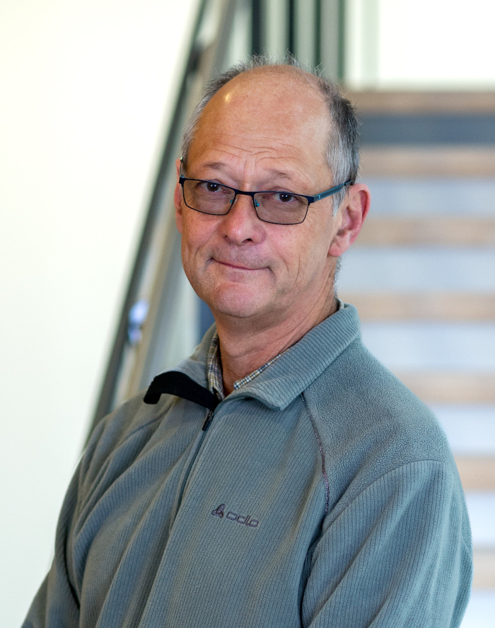
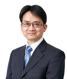
11:35 – 12:00 Atsushi Ogura – Meiji University: Process Technologies for 3-dimensional COMS Integrated Circuits
Abstract
Recent advancements in large-scale integration (LSI) have been achieved through a combination of saturating miniaturisation and accelerated adoption of three-dimensional (3D) structures. This presentation will introduce several key technologies from advanced manufacturing processes that are essential for 3D complementary metal–oxide–semiconductor (CMOS) integrated circuits. It will review and discuss the current status of these technologies and the associated challenges.
Bio - Atsushi Ogura
Atsushi Ogura received the B.S. and the M.S. from Waseda University, Tokyo, Japan, in 1982 and 1984, respectively. He received Ph.D. degree in engineering in 1991 also from Waseda University.
He joined Fundamental Research Laboratories, NEC Corporation, Kawasaki, Japan, where he has been engaged in the research on fabrication and evaluation of SOI materials. He was a Visiting Researcher at AT&T Bell Laboratories, NJ, from 1992 to 1994. He left NEC in 2004. Presently he is a professor of Meiji University with main research subjects of science in Si materials and processes for LSI and Photovoltaic applications.
12:00 – 13:35 | Lunch break
- 13:35-14:25
Session 3 – Policy session
13:35 - 14:00 | Europe’s semiconductor strategy - Olivier Brigner, European Commission
14:00- 14:25 | Japan’s semiconductor strategy - Tomoshige Nambu, METI
11:35 – 12:00 Atsushi Ogura – Meiji University: Process Technologies for 3-dimensional COMS Integrated Circuits
Abstract
Recent advancements in large-scale integration (LSI) have been achieved through a combination of saturating miniaturisation and accelerated adoption of three-dimensional (3D) structures. This presentation will introduce several key technologies from advanced manufacturing processes that are essential for 3D complementary metal–oxide–semiconductor (CMOS) integrated circuits. It will review and discuss the current status of these technologies and the associated challenges.
Bio - Atsushi Ogura
Atsushi Ogura received the B.S. and the M.S. from Waseda University, Tokyo, Japan, in 1982 and 1984, respectively. He received Ph.D. degree in engineering in 1991 also from Waseda University.
He joined Fundamental Research Laboratories, NEC Corporation, Kawasaki, Japan, where he has been engaged in the research on fabrication and evaluation of SOI materials. He was a Visiting Researcher at AT&T Bell Laboratories, NJ, from 1992 to 1994. He left NEC in 2004. Presently he is a professor of Meiji University with main research subjects of science in Si materials and processes for LSI and Photovoltaic applications.
- 14:25–15:40
Session 4 – Energy Harvesting
14:25 - 14:50 | ZnO thin films and nanowires for piezoelectric energy transducer applications - Gustavo Ardila, University Grenoble-Alpes
Abstract
Piezoelectric thin films are widely used in MEMS and NEMS actuators and resonators, but also in mechanical sensors and energy harvesters for IoT applications and Wireless Sensors Networks. Piezoelectric nanowires (NWs) and their integration into nanocomposites are an alternative to thin films with nanostructuration benefits. Zinc oxide (ZnO) is an excellent candidate for the fabrication of such structures thanks to its low-cost and environment friendly fabrication process. This presentation will cover some recent developments on ZnO thin films, NWs and their integration into devices. The discussion will cover the electromechanical characterization of these structures and the confrontation with theoretical simulations.
Bio - Gustavo Ardila
Gustavo Ardila received his BS in electronic engineering and physics from the University of Andes, Colombia in 2002 and 2003, respectively, and his MS in microelectronic and microsystems circuit conception from the National Institute of Applied Science (INSA) in Toulouse, France in 2004. He received his PhD degree in Electrical Engineering in 2008 from the Paul Sabatier University in Toulouse. After 1 year of postdoctoral position in LAAS-CNRS laboratory in Toulouse, in 2009 he became Associate Professor at the Grenoble Alpes University and a researcher at CROMA, Grenoble, France. He is or was involved in several French and European projects related to energy harvesting or sensing applications using piezoelectric materials. He presently leads the European team to develop the Roadmap of Energy Harvesting technologies contributing to the IEEE IRDS (International Roadmap for Devices and Systems). He is member of the editorial board of the “Energy” section of ISTE-Wiley publisher.
14:50 - 15:15 | Thermoelectric energy harvesting and cooling technology; New developments - Takao Mori, NIMS:
Abstract
Thermoelectric materials can be used for various energy harvesting power generation applications, or solid-state cooling. We have been utilizing novel routes such as magnetism, Anderson localization, defect engineering, etc. to overcome traditional physical properties tradeoffs and achieve high thermoelectric performance. As a result, we have succeeded in developing novel materials & modules that surpass the half-century champion Bi2Te3-type. Electrode technologies for these new materials were also developed, with a novel concept of “active electrodes” leading to high stability and enhancement of the device performance, also for diffusion barrier materials. Effective methodology for designing high performance thermoelectric modules (TEGs) has also been developed. Accurate evaluation of performance of actual devices is critical for industrialization, and we have also laid out the best practices for evaluation of TEGs. We also made advancements in fabrication of various formats of TEGs: bulk, thin film, flexible. Thermal management technologies are also being developed. Cooling is becoming increasingly critical for data centers and the semiconductor industry, and we have also fabricated Peltier devices of novel materials, together with developing viable active cooling materials to realise the next generation cooling. Support from JST Mirai Large-Scale Program JPMJMI19A1 is acknowledged.
Bio - Takao Mori
Takao Mori received his PhD at U. Tokyo, Dept. Physics. He is a Field Director at National Institute for Materials Science (NIMS) and Professor of U. Tsukuba Graduate School, and elected Board Member, present President of the International Thermoelectric Society (ITS). Mori’s research interests are, broadly speaking, to find ways to control structures and properties of inorganic materials. He is especially involved in development of thermoelectric materials and multidisciplinary enhancement principles, such as utilizing magnetism, in order to find new routes to achieve high control over band structures and electrical and thermal transport. And furthermore, working on thermoelectric devices, module and thermal management technology for applications. Mori is a Senior Editor of Materials Today Physics, Advisory Board Member of JSSC, J. Materiomics, PRX Energy, Joule, Device. He is a Program Manager of JST Mirai Large-scale Program. Mori has published over 500 papers, 25 book chapters, 40 patents.
15:15 - 15:40 | Tailoring the Physical Properties of Narrow-Gap Semiconductor Mg2S Thermoelectric Thin Films through Defect Engineering - Takeaki Sakurai, University of Tsukuba
Abstract
Thin-film-based miniature thermoelectric (TE) devices are attracting attention for Internet of Things (IoT) applications because they can effectively recover waste heat generated within electronic components. Among various thermoelectric materials, Mg2Sn and related Mg2(Sn,Ge) compounds are considered promising low-cost candidates that perform well in the temperature range near room temperature. This study explores the enhancement of thermoelectric properties in p-type Mg2Sn-based epitaxial thin films through defect engineering and doping strategies. By optimizing the synthesis process and precisely incorporating dopants, significant improvements in both electrical and thermoelectric performance were achieved. The control of defect structures with Ge incorporation and Mg flux modulation, such as vacancies and stacking faults, played a crucial role in modulating phonon scattering and charge transport, leading to enhanced thermoelectric efficiency. Doping strategies, particularly the introduction of Li for p-type conductivity, proved essential in balancing electrical conductivity and the Seebeck coefficient. These findings underscore the importance of combining precise doping control and defect management to develop high-performance thermoelectric materials. This work hopes to provide valuable insights for advancing the design and optimization of Mg2Sn-based systems, making them more suitable for next-generation energy-harvesting applications.
Bio - Atsushi Ogura
Dr. Takeaki Sakurai is an Executive Officer and Professor at University of Tsukuba, Japan. His research focuses on compound semiconductor materials and their application to high-efficiency solar, thermal, and chemical energy conversion devices. He also oversees the coordination of international collaborative projects in his executive role.
15:40 – 16:00 | Coffee break
- 16:00-16:50
Session 5 – Quantum Computing
16:00 - 16:25 | : Quantum Computing using Si-based Qubits - Jean-Charles Barbe, Quobly
16:25 - 16:50 | High-fidelity of spin Qubits in silicon - Seigo Tarucha, RIKEN
Abstract
Over the past two decades, research on quantum computing (QC) has advanced rapidly from theory to experiment across multiple hardware platforms. Among them, quantum dot (QD)–based QC, although initiated later than others, has recently attracted momentum because they combine a compact footprint with compatibility with advanced semiconductor manufacturing. Major players, including Intel, imec, and CEA-Leti, are now actively developing semiconductor qubits.
Our work investigates silicon QDs that host electron spin qubits, bridging device physics and QC applications. Critical hurdles toward practical processors include high-fidelity, fault-tolerant operation, quantum error correction, and scalable architecture. We implement spin qubits in isotopically purified Si/SiGe QDs with an integrated micromagnet and demonstrate single- and two-qubit gates with fidelities, meeting typical thresholds for fault-tolerant quantum computation. In this talk, I will review recent advances in qubit performance, error generation and their correction, and system-level approaches to scaling spin-qubit arrays.
Bio - Seigo Tarucha
Seigo Tarucha received the B. E. and M. S. degrees from the University of Tokyo in 1976 and 1978, respectively. He joined NTT in 1978 and received the Ph. D degree in applied physics from the University of Tokyo in 1986. In 1998 he moved to the University of Tokyo as a professor in the Phys. Dept. and then to the Appl. Phys. Dept. in 2004. In 2019 he retired from the University of Tokyo and since then has been fully affiliated to RIKEN Center for Emergent Matter Science (CEMS). He has been running a research group in CEMS since 2012 and additionally a research team in Center for Quantum Computing (RQC) since 2021. His current research interests have focused on spin-based quantum computing. He received Kubo Ryogo award, Nishina award in 2002, National medal with purple ribbon in 2004, Leo Esaki Award in 2007, Achievement award of Japan Applied Physics Society in 2018, and Fujiwara Award in 2023.
- 16:50-17:40
Session 6 – Neuromorphic Computing
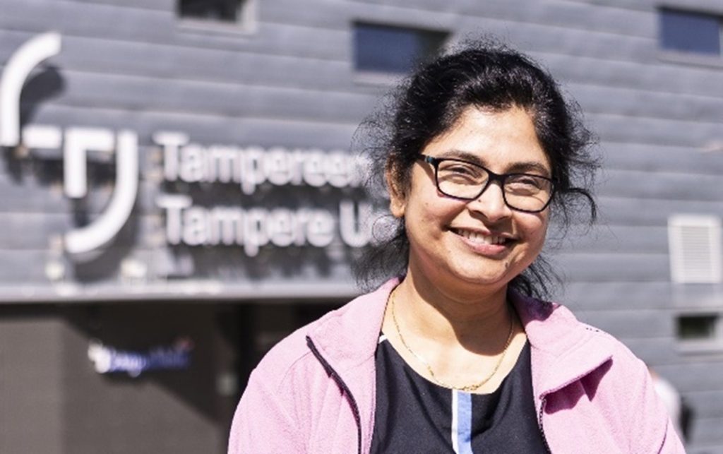
16:50 - 17:15 | Neuromorphic Electronics for Intelligence Everywhere - Sayani Majumdar, Tampere University
Abstract
Unprecedented advances in Artificial Intelligence (AI)-assisted automation continue to drive the demand for novel hardware that is significantly more scalable, compact, and energy-efficient as the exponentially rising demand for computational and electrical power is becoming unsustainable. Data centers consumed approximately 415 terawatt-hours (TWh), 1.5% of the world’s electricity in 2024, and projected to consume 945 TWh by 2030, driven largely by AI. Neuromorphic computing, inspired by the event-driven and massively parallel information processing ability of the human brain, offers a compelling solution, especially as emerging device technologies now enable true in-memory computation and tightly integrated sensing capabilities far beyond what CMOS alone can achieve.
In recent years, Europe has emerged as a global hotspot for neuromorphic computing research, driven by pioneering research, a strong academic-industrial ecosystem, and a strategic focus on energy-efficient, brain-inspired hardware to advance edge AI. While SpiNNaker in UK and BrainScaleS in Germany provides essential large-infrastructure and data for brain-inspired research, strong strategic partnership between research organizations and industry in multiple EU projects is advancing this field at a rapid pace, especially to bring neuromorphic AI at the edge. However, more strategic international collaboration with advanced semiconductor countries is needed for large-scale deployment of the neuromorphic hardware to bring human brain-level processing complexity in silicon.
In this talk, I will present an overview of the field of Neuromorphic computing and sensing highlighting the progress and path forward for the next-generation neuromorphic AI hardware that will enable deployment of this technology in resource-constrained edge platforms, such as wearable health monitoring, soft robotics, and autonomous embedded sensing systems. Lastly, I will discuss the need for embracing a full-stack co-optimization strategy from advanced materials and devices to circuits, architectures, and learning algorithms and need for international collaboration that can ultimately enable adaptive, autonomous computing systems embedded seamlessly into everyday environments, making the vision for intelligence everywhere a reality.
Bio - Sayani Majumdar
Dr. Sayani Majumdar is an Associate Professor of Electrical Engineering at the Faculty of Information Technologies and Communication Sciences at Tampere University, Finland. She is also a visiting professor at the Miin Wu School of Computing at National Cheng Kung University, Taiwan. Her career in semiconductor device research spans more than two decades where she worked in both academia and in close collaboration with the industry. She worked on several emerging technologies in world-leading organizations including MIT, USA and Max-Planck Institute, Germany. Her team’s current research focuses on the development of embedded non-volatile memories and neuromorphic computing hardware using low-thermal budget ferroelectric and semiconductor materials and processes for their back-end-of-line integration with CMOS circuits for their application in low-power neuromorphic edge devices.
17:15 - 17:40 | Physical Reservoir Computing Utilizing HfO2-based Ferroelectric Devices for Edge-AI Applications - Shinichi Takagi, Teikyo University
Abstract
The rising demand for energy-efficient AI computing has intensified research into technologies that optimize both performance and power consumption. Processing real-time time-series data at the edge remains a critical challenge, traditionally addressed by recurrent neural networks (RNNs). Reservoir Computing (RC), a specialized RNN, offers a low-learning-cost alternative by utilizing a “reservoir” with fixed weights, where only the readout layer requires optimization. This presentation highlights physical RC using HfO2-based ferroelectric gate field-effect transistors (FeFETs) and MFM capacitors. By leveraging the inherent nonlinear dynamics and short-term memory of spontaneous polarization, these devices functionally transcend conventional nonvolatile memory. The ferroelectric device reservoir provides following three distinct advantages: (1) nonlinearity derived from the interaction between channel carriers and polarization (2) full compatibility with standard silicon fabrication processes (3) seamless integration with Si CMOS circuits. We will discuss the fundamental principles of FeFET-based RC, techniques for performance enhancement, and recent advances in practical application examples. This hardware-intrinsic approach provides a scalable, Si-platform-compatible solution for high-efficiency neuromorphic computing at the edge.
Bio - Shinichi Takagi
Shinichi Takagi received the B.S., M.S. and Ph.D. degrees in electronic engineering from the University of Tokyo, Tokyo, Japan, in 1982, 1984 and 1987, respectively. He joined the Toshiba Research and Development Center, Kawasaki, Japan, in 1987. From 1993 to 1995, he was a Visiting Scholar at Stanford University, Stanford, CA. In 2003, he moved to the University of Tokyo, where he worked as a professor in the department of Electrical Engineering and Information Systems, School of Engineering. Since 2025, he has been working as a Specially Appointed Professor in Advanced Comprehensive Research Organization, Teikyo University, Tokyo, Japan. He has been engaged in research of Si MOS device physics and the development of novel CMOS devices. He received 22 awards including IEEE Paul Rappaport Award (2014), IEEE Andrew S. Grove Award (2013), and IEEE George E. Smith Award (2003).
Networking cocktail
Day 2 : 25 March
- 8:45-10:00
Session 1 – Heterogeneous Integration and Advanced Packaging
8:45 - 9:10 | Applied Research in 3d Heterogeneous Integration and Advanced Packaging of Next Generation Semiconductor Products - Patrick Bressler, Fraunhofer
Abstract
The Research Factory Microelectronics Germany – FMD – is an initiative of the German Research Ministry with 11 Fraunhofer Institutes and 2 Leibniz Institutes to coordinate joint-research in the field of microelectronics in Germany. The European Pilot Line for Advanced Packaging and Heterogeneous Integration for Electronics Components and Systems (APECS), a distributed pilot line across Europe with 10 research partners in 8 European Union Member States coordinated by the FMD, aims to accelerate technology innovation and market deployment in 3D Heterogeneous Integration and Advanced Packaging. The pilot line is open for collaborative research projects with third-party partners.
Bio - Patrick Bressler
Dr. Patrick Bressler is the director for international cooperation, emerging technologies and innovation at the Fraunhofer Microelectronics Group / FMD (Research-Fab Microelectronics Germany). Responsibilities include technology evaluation, partnerships for research, innovation and work force development, and advancing European and international R&D&I programmes, including the APECS pilot lines. A semiconductor and surface physicist by training, Patrick also serves as the General Secretary of the European Materials Research Society, E MRS, based in Strasbourg.
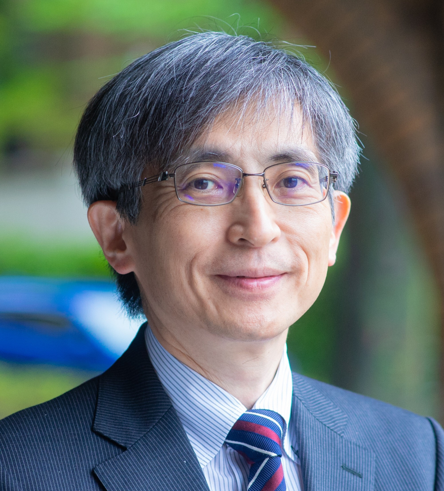
9:10 - 9:35 | Interconnects for AI in the 3D Chiplet Era: Japan’s Ecosystem View - Fumihiro Inoue, Yokohama National University
Abstract
Interconnect technologies are becoming a defining factor in AI system performance in the 3D chiplet era. As scaling limits, power delivery, memory bandwidth, thermal management, and heterogeneous integration increasingly determine system capability, advanced packaging is shifting from a backend process to a central innovation driver. This talk discusses how interconnects, including hybrid bonding, fine-pitch redistribution, and chiplet-level integration, are reshaping the design and manufacturing landscape for AI hardware. Beyond the technology itself, the lecture highlights the importance of ecosystem formation: aligning materials, equipment, process integration, design, reliability evaluation, and talent development across organizational boundaries. From Japan’s perspective, this transition presents both a challenge and an opportunity. By leveraging its strengths in materials, precision manufacturing, and collaborative industrial networks, Japan can play a distinctive role in building the next generation of AI hardware platforms. The talk offers an ecosystem-level view of where technical bottlenecks remain and where strategic value can be created.
Bio - Shinichi Takagi
Fumihiro Inoue is an Associate Professor at Yokohama National University, specializing in 3D integration and chiplet. Before joining the university, he contributed extensively to advancing unit processes for 3D integration during his role as researcher at imec, which lasted until 2021. In recognition of his significant contributions to the field, he received the prestigious IEEE EPS Outstanding Young Engineer Award in 2022. Since April 2024, Dr. Inoue has also served as the Vice-Director of the Semiconductor and Quantum Integrated Electronics Research Center at Yokohama National University, where he continues to lead cutting-edge research initiatives.
9:35 - 10:00 | Wafer-Scale 3D Photonic Chiplet Integration for AI System - Koyanagi Mitsumasa, Tohoku University
Abstract
A new self-assembly technology to three-dimensionally integrate AI chip, memory chip and photonic chip is described. Many AI chips and memory chips are connected by optical waveguides through a wafer which are driven by photonic chips.
Bio - Koyanagi Mitsumasa
He received the Ph.D. degree from Tohoku University in 1974 and then joined Hitachi Ltd. where he invented a stacked capacitor DRAM memory cell which has been widely used in the DRAM production. In 1985, he joined the Xerox Palo Alto Research Center where he worked on sub-micron CMOS devices. In 1988 he joined Hiroshima University where he worked on sub-0.1um MOS devices, 3D integration technology, optical interconnection and parallel computer system. He proposed 3D integration technology using TSV for the first time in 1989. In 1994, he joined Tohoku University where he succeeded in fabricating the first 3D stacked image sensor in 1999, the first 3D stacked DRAM in 2000 and the first 3D stacked processor in 2002. He established a small production line for 3D integration using 12-inch wafers called GINTI (Global Integration Initiative) in 2013 and became a director. Currently he is a senior research fellow in New Industry Creation Hatchery Center (NICHe), Tohoku University and CTO in Tohoku Microtec Co. Ltd. He has published more than 400 technical papers and given more than 200 invited and keynote speeches. He was awarded IEEE Jun-ichi Nishizawa Medal, IEEE Cledo Brunetti Award, SSDM Award and Okouchi Memorial Prize owing to the invention of stacked capacitor DRAM memory device. In addition, he was awarded IEEE Rao Tummala Award and 3DIC Pioneer Award by his pioneering works in 3D integration technology. He was also awarded Optoelectronic Technology Achievement Award from Japan Society of Applied Physics. Furthermore, owing to his overall contribution to the progress of semiconductor technology he was awarded the National Medal Order of the Sacred Treasure, the National Medal with Purple Ribbon, the Award of Ministry of Education, Culture, Sports, Science and Technology and JSAP Outstanding Achievement Award. He is an IEEE life fellow and a JSAP fellow.
10:00 – 10:15 | Coffee Break
- 10:15-11:30
Session 2 – New Channel Materials
10:15 - 10:40 | Polycrystalline Germanium as a High-Mobility Channel Material for Thin-Film Transistors - Kaoru Toko, University of Tsukuba
Abstract
Low-temperature formation of high-performance semiconductor thin films on insulating substrates is a key technology for integrating functional devices into silicon large-scale integrated circuits, flat-panel displays, and a wide variety of sensors. Ge-based semiconductors, including SiGe and GeSn alloys, exhibit higher carrier mobility and lower crystallization temperature than silicon while maintaining compatibility with established silicon technologies. Because their narrow band gap can cause leakage current in bulk structures, thin-film structures are particularly attractive. These characteristics make Ge-based thin films promising channel materials for next-generation thin-film transistors. However, device performance has been limited by the crystallinity of the Ge layer itself.
We discovered that increasing the atomic density of an amorphous Ge precursor dramatically enhances grain growth during solid-phase crystallization at temperatures below 500 °C. This approach enables polycrystalline Ge films on insulating substrates with hole mobility exceeding that of single-crystal Si. The resulting transistors exhibit the highest reported performance among Ge thin-film transistors formed at such low temperatures, and the process also enables fabrication on flexible plastic substrates.
In this presentation, I will introduce our recent progress in Ge-based thin films, covering topics from crystallization mechanisms to thin-film transistor performance.
Bio - Kaoru Toko
Kaoru Toko is a Professor in the Faculty of Pure and Applied Sciences at the University of Tsukuba, Japan. He received his Ph.D. in Engineering from Kyushu University in 2011 and joined the University of Tsukuba the same year. His research focuses on the low-temperature synthesis of high-performance semiconductor thin films, particularly polycrystalline germanium and related alloys, for thin-film electronics and flexible devices. He has authored more than 300 peer-reviewed publications in this research area.
10:40 - 11:05 | 2D channel materials - Burkay Uzlu, AMO
Abstract
Bio - Burkay Uzlu
11:05 - 11:30 | Resistance Switch in a Minimal-Fullerene devices - Kazuhito Tsukagoshi, NMS
Abstract
Electromechanical switching in fullerene C60 nanochains, introduced in the device as a C60 pyrrolidine tris-acid film, was realized in nanogap electrodes with ~20-nm separation, where negative differential resistance and binary resistance switching were reproducibly observed. In the nanogap electrodes, an initial conductive C60 chain spontaneously formed only through a direct current injection from the electrode without any preset process of electron beam irradiation on the C60 channel film, which was always needed for microscale C60 channels. The nanoscale C60 chain in the nanogap allowed us to evaluate the single junction resistance in the switching cycle. From the switching voltage and current values, the switching energy for the C60 chain in the nanogap was estimated to be approximately several milliwatts, most probably caused by the polymerization and depolymerization of the conductive C60 chain. These novel results provide significant advantages for electron device development over the commonly used STM tool.
Bio - Kazuhito Tsukagoshi
2009~present, PI, MANA, NIMS
2008, Senior Researcher, AIST
2009~2010, Reseracher/Research unit leader, RIKEN
Ph. D., Dep. Physics., 1993~1995, Graduate school of Science, Osaka University, Japan
M. S., Dep. Physics., 1990~1992, Graduate school of Science, Osaka University, Japan
B. S., Dep. Physics., 1986~1990, Nagoya University, Japan
- 11:30-12:20
Session 3 – Semiconductor technology, value chain and projects for possible international cooperation
11:30 - 11:55 | Semiconductor technologies, value chain and projects for possible international cooperation - Francis Balestra, CNRS
Abstract
International cooperation is key for knowledge exchange, speeding up technological innovation, reducing cost by avoiding duplicated research, boosting the resilience of the semiconductor value chains, manage risks due to the turbulent geopolitical context, reduce skills shortage, overcome gaps in standardisation, strengthen Europe’s and Japan’s position in the semiconductor area representing pivotal technologies for almost all existing industrial sectors, and is encouraged by the new strategies of leading semiconductor countries. This presentation will deal with the analysis of the semiconductor economic and technological landscapes and value chains, the identification of the most promising emerging technologies, the main challenges and opportunities for bilateral Japan-EU collaborations in the fields of advanced functionalities and computing, and possible projects for international cooperation.
Bio - Francis Balestra
BALESTRA Francis, CNRS Research Director at CROMA, is Director Emeritus of the European SiNANO Institute and Chair of IEEE Electron Device Society France, and has been Director of several Research labs. He coordinated many European Projects (ICOS, NEREID, NANOFUNCTION, NANOSIL, etc.) that have represented unprecedented collaborations in Europe in the field of Nanoelectronics. He founded and/or organized over 50 international Conferences and Workshops, and has co-authored more than 500 publications. He is member of several European Scientific Councils, of the Advisory Committees of International Journals and of the IRDS (International Roadmap for Devices and Systems) International Roadmap Committee as representative of Europe.
11:55 - 12:20 | Crypto Hardware Accelerator Design and Rapid Chips Design & Fabrication Platform - Makoto Ikeda, University of Tokyo
Abstract
Bio - Burkay Uzlu
12:20 – 13:30 | Lunch Break
- 13:30-13:55
Session 4 – Power devices
13:30 - 13:55 | Gallium oxide power device technologies - Masataka Higashiwaki, Osaka Metropolitan University
Abstract
We have been conducting research and development of Ga2O3 FETs and diodes for over 15 years. Many of the fundamental technologies for Ga2O3 power devices have been established, which are currently in the stage of transferring the technologies to industry and then moving on to full-scale device development aimed at commercialization and practical applications based on the transferred technologies. In this talk, our recent research topics on Ga2O3 FinFETs and molecular beam epitaxy growth of nitrogen (N)-doped Ga2O3 thin films will be discussed.
It is well known that N atoms doped in Ga2O3 function as deep acceptors, and that an energy barrier of about 3 eV can be formed at the N-doped Ga2O3/n-Ga2O3 junction. Recently, we found that N radical irradiation is effective to recover n-Ga2O3 surface damage and improve electrical properties of Schottky interfaces. Ga2O3 FinFETs fabricated with the N radical irradiation revealed improvement of in-plane uniformities of device characteristics and a positive shift of a threshold gate voltage. Furthermore, high-density N-doped Ga2O3/n-Ga2O3 heterostructures grown by MBE showed unique electrical properties depending on the density, which were provided by highly activated N deep acceptors. We believe that the N doping can be one of the key process technologies for future development of Ga2O3 devices.
Bio - Masataka Higashiwaki
Masataka Higashiwaki is currently a Professor of the Department of Physics and Electronics, Osaka Metropolitan University, and a Director of Green ICT Device Laboratory, the National Institute of Information and Communications Technology. His current research interest is in Ga2O3 device and material engineering. His research is recognized by awards such as the 2007 International Symposium on Compound Semiconductors (ISCS) Young Scientist Award, and the 2021, 2023, and 2024 Clarivate Highly Cited Researcher. He has authored or co-authored more than 150 papers in peer-reviewed journals and has given more than 140 invited talks at international conferences. He is a Fellow of the IEEE.
13:55 - 14:20 | Widebandgap and ultrawide-bandgap power - Andrea Tallarico, University of Bologna
Abstract
Bio - Andrea Tallarico
- 14:20-15:10
Session 5 – Memory Technologies
14:20 - 14:45 | DFT and Quantum Transport Simulations of 2D Material-Based Resistive Memories - Alessandro Cresti, CNRS
Abstract
2D materials, characterized by their tunable electronic properties, atomic thinness, and mechanical flexibility, hold significant promise for the development of low-power, high-durability devices. Among these, atomristors—nonvolatile resistive memory devices composed of few-layer 2D materials sandwiched between metallic contacts—have emerged as versatile components with applications ranging from RF switches to neuromorphic computing. Their operational mechanisms, however, involve complex and concurrent physical processes that remain only partially understood.
I will present density functional theory and quantum transport simulations of both pristine and defected atomristors, exploring the role of different metallic contacts and 2D materials. While our models intentionally simplify the experimental complexity, they provide valuable insights to guide the interpretation of experimental data and inform the rational design of next-generation devices. Our ongoing research and perspectives, for which international collaborations are more than welcome, further extend these simulations to fully 2D ferromagnetic and ferroelectric memories, opening new avenues for ultra-low-power, multifunctional electronics.
Bio - Alessandro Cresti
Alessandro Cresti is a researcher at the French National Center for Scientific Research (CNRS), where he leads cutting-edge research in quantum transport simulations and emerging electronic technologies. With a Ph.D. in Physics from the University of Pisa (2006), he has almost 20 years of experience in the theoretical and computational study of nanoscale electronic devices, with a focus on 2D materials such as graphene and transition metal dichalcogenides.
His work centers on developing advanced full-quantum simulation tools to explore fundamental and applied aspects of electronic transport in nanostructures. He investigates innovative materials and device architectures for next-generation memory and logic applications, bridging the gap between theoretical insights and experimental advancements.
He also served as the scientific coordinator of the book « Beyond-CMOS: State of the Art and Trends », a comprehensive reference on the physics and future prospects of emerging electronic technologies.
14:45 - 15:10 | Low Power Nonvolatile NBFPGA for Space and Cryogenic Applications - Muneihiro Tada, Keio University
Abstract
This presentation introduces a Low Power Nonvolatile NanoBridge FPGA (NBFPGA) designed to operate reliably in the extreme environments of space and cryogenic temperatures. Conventional FPGAs face significant challenges in these settings, including high power leakage, radiation-induced soft errors, and performance degradation.
Our research leverages the unique characteristics of NanoBridge technology, which utilizes metallic filament growth and dissolution to achieve nonvolatility and high radiation hardness. By integrating these atom-switch-based devices, the NBFPGA eliminates configuration memory leakage and provides an inherently “instant-on” capability.
Furthermore, we discuss the hardware’s robust performance at cryogenic temperatures, a critical requirement for controlling quantum processors and deep-space instruments. The synergy between new materials and specialized circuit architecture allows for a significant improvement in energy efficiency without relying solely on CMOS scaling. We cover the full design spectrum from material-level reliability to circuit-level optimization, demonstrating that the NBFPGA is a key enabling technology for the next generation of power-constrained, high-reliability autonomous systems in extreme frontiers.
Bio - Munehiro Tada
Munehiro Tada received the M.S. and Ph.D. degrees from Keio University, Japan. He joined NEC Corporation in 1999. From 2007 to 2008, he was a visiting scholar at Stanford University. From 2019, he is a cofounder and executive board director at NanoBridge Semiconductor, Inc. From 2024, he is a full professor at Keio University.
He published papers with 16-IEDM, 17-VLSI and 11-IITC. He hold more than 100 issued patents. He is an IEEE Fellow and a JSAP Fellow. He is an adviser at JST-CREST(2020-), an executive board director at JSAP (2024-2025), a board director at NanoBridge Semiconductor, Inc.(2019-), a director at Yagami Innovation Laboratory in Keio University (2025-), and IEEE Fellow Committee Member (2026-).
15:10 – 15:25 | Coffee Break
- 15:25-16:15
Session 6 – Optoelectronics
15:25 - 15:50 | Semiconductor-based photonics and optoelectronics - Abdul Rahim, PhotonDelta
Abstract
Bio - Abdul Rahim
15:50 - 16:15 | Photonic Integrated Circuits with Heterogeneous Material Integration and Photonics - Nobuhiko Nishiyama, Institute of Science Tokyo
Abstract
Bio - Munehiro Tada
- 16:15-16:40
Session 7 – International Cooperation
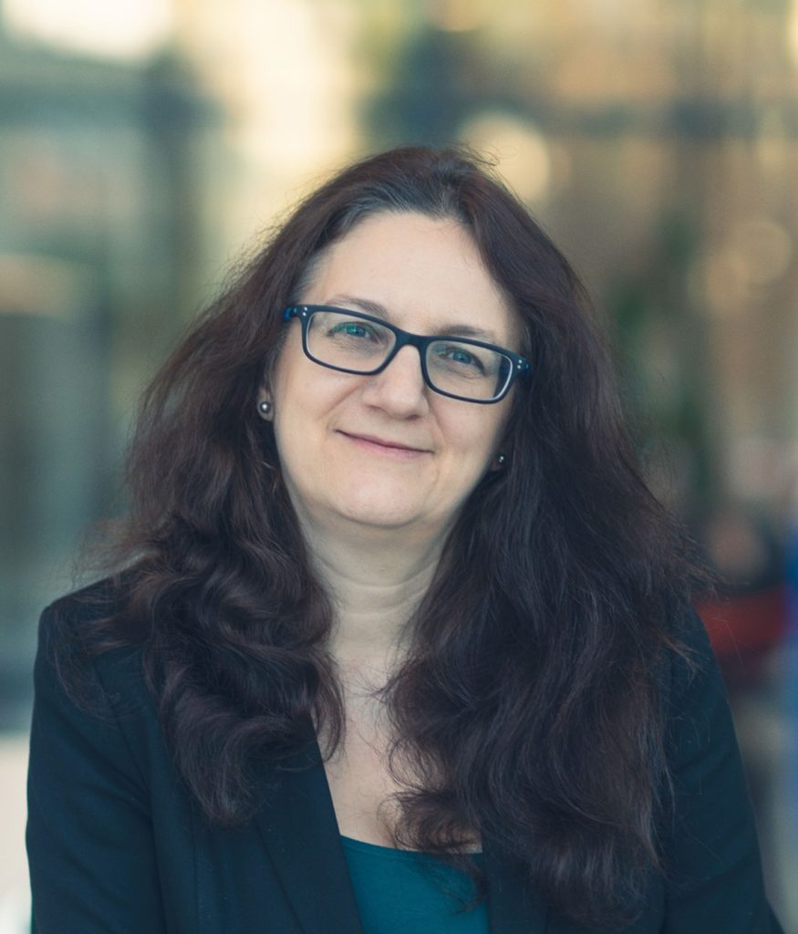
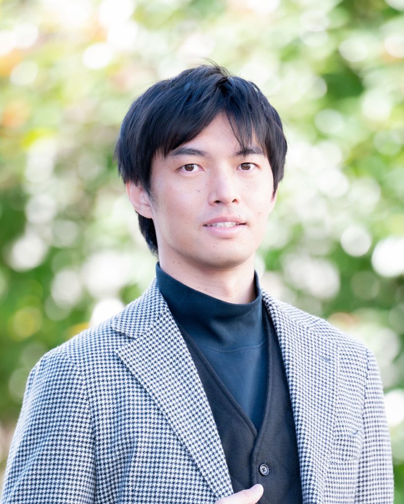
16:15 - 16:40 | Japan-EU JASMINE Chips Project - Mircea Modreanu – Tyndall National Institute
Abstract
The JASMINE (Japan and EU Semiconductors: Mutual Innovation & Excellence) initiative plays a strategic role in supporting the European Commission’s ambition to strengthen Europe’s global position in the semiconductor value chain, as outlined in the European Chips Act. Its core mission is to identify priority areas where research cooperation with Japan will accelerate technological leadership, enhance industrial competitiveness, and contribute to a resilient, sustainable semiconductor ecosystem.
The project proposes a strategic EU‑Japan framework built on complementary capabilities: Japan’s world‑class expertise in materials, manufacturing equipment, and advanced packaging, combined with the EU’s leadership in fundamental research, photonics, quantum technologies, and high‑value application domains. By leveraging these synergies, JASMINE aims to accelerate co‑innovation, enhance industrial resilience, and help both regions strengthen their semiconductor ecosystems in an increasingly competitive global landscape. Building on an in‑depth analysis of (a) the structure and evolution of global semiconductor value chains, (b) the strengths and strategic gaps of European industry, and (c) opportunities presented by next‑generation and emerging technologies, JASMINE will identify a set of targeted bilateral and multilateral research directions with Japan.
Bio - Mircea Modreanu
Dr. Mircea Modreanu is a leading European expert in nanomaterials and semiconductor technologies, serving as Principal Investigator at the Tyndall National Institute since 2002. He holds a PhD in Physics from the University of Bucharest and has strengthened his international profile through Visiting Professor Fellowships at INP Grenoble (France) and two JSPS Professor fellowships in Japan. His research focuses on advanced materials for micro‑/nano‑electronics, nanophotonics, and RF to millimeter‑wave systems—core technologies underpinning Europe‑Japan digital innovation, connectivity, and semiconductor resilience. He is also widely recognized for his expertise in optical spectroscopy and advanced material characterization.
Dr. Modreanu coordinates the CHIPS JU JASMINE project, a flagship initiative enhancing EU‑Japan cooperation in semiconductor materials and device innovation. He previously led the EIC project Nano‑EH, advancing smart energy‑harvesting materials for the future Internet of Things, and is currently Principal Investigator for the Horizon Europe Powersat project, developing hybrid solar–microwave energy‑harvesting for next‑generation satellite‑based digital services. He has secured 12 competitive research grants, chaired 12 international conferences across Europe and Japan, published over 175 scientific papers, and has three patent applications pending.
- 16:40-17:05
Plenary
Light-weight Molecular Sensor for IoT Society - Atsuyoshi Koike, Rapidus
Abstract
As the demand for AI-driven technologies continues to surge, the semiconductor industry has entered a critical turning point. This presentation introduces Rapidus and its mission to redefine the logic chip landscape through unprecedented speed and international synergy.
Central to our strategy is a direct response to new market needs—the urgent requirement for Short Turnaround Time (TAT) to support the rapid design and manufacturing of diverse, high-end semiconductors. To address this, Rapidus introduces an innovative business model: RUMS (Rapid-Unified Manufacturing Service). By leveraging a fully single-wafer processing system, we offer an agile manufacturing alternative that moves beyond traditional batch-based production.
Finally, we discuss our role in the new world order and the risks posed by global supply-demand gaps. Rapidus is committed to building a resilient ecosystem through deep global collaboration with leading research institutions and enterprises, particularly across Europe and beyond. Together, we aim to establish a rapid, reliable foundation for the future of cutting-edge semiconductors.
Bio - Atsuyoshi Koike
Atsuyoshi Koike, Ph.D.
CEO, Rapidus Corporation
ATSUYOSHI KOIKE established Rapidus Corporation, a company that researches, develops, designs, manufactures, and sells advanced logic semiconductors, in August 2022.
Prior to the current role, Koike had served as President of Western Digital Japan since April 2018. Prior to joining Western Digital, he served as corporate chief engineer for Renesas Technology Corporation. Previously, he held the position of president and chief executive officer, as well as other senior leadership positions at Trecenti Technologies, Inc. Prior to that, he held senior manufacturing management and executive leadership positions at Hitachi, Ltd.
Koike received the B.S. and M.S. in Materials Science and Engineering from Waseda University and Ph.D. in Electronic Engineering from Tohoku University. He is a Professor and Special Senior Advisor at Tohoku University of New Industry Creation Hatchery Center, and has given lectures at the University of Tokyo.
- 17:05-17:20
Closing Remarks - Ken Uchida
Bio - Ken Uchida
Ken Uchida received the B.S. degree in Physics, M.S. and Ph.D. degrees in Applied Physics from The University of Tokyo, Japan, in 1993, 1995 and 2002, respectively. In 1995, he joined the R&D Center of Toshiba Corporation. In 2008, he moved to Tokyo Institute of Technology as an associate professor. In 2012, he moved to Keio University, as a full professor, and then to the University of Tokyo, as a full professor. He has studied the physics of nanoscale devices.
- Agenda
Other events
Workshops, conferences and meetings of the JASMINE network
Mar 24
Upon registration
- Conference
2nd EU-JAPAN DIGITAL WEEK 2026
Japan-EU Cooperation on Advanced Computing & Functionalities, Heterogeneous Integration and Semiconductor Value Chain
- School of Engineering, University of Tokyo, Japan
- 200+ participants
Our partners
INPACE Hub
About this partner
INPACE’s mission is to support the implementation of the Digital Partnerships between the European Union and Japan, South Korea, Singapore, as well as the Trade and Technology Council with India.
Powered by a consortium of 21 European and Asian partners, the initiative establishes a multi-stakeholder Hub for collaboration in digital technologies between Europe and the Indo-Pacific region and fosters long-term cooperation in key digital technologies by bringing together experts and stakeholders from both regions.
- Association
SiNANO Institute
?? France
About this partner
The SINANO Institute is the European Academic and Scientific Association for Nanoelectronics, connecting the European Research and Academic community in semiconductor science and technologies. It gathers 27 academic/RTO members and 22 deep-tech start-ups from 16 European Countries. The SINANO mission is to secure the future of European semiconductor science and technology by mobilizing and nurturing the European R&I community, promoting and strengthening synergies in the field through our membership, accelerating the translation of excellent research into European knowhow, technologies, and products, ensuring the pipeline of talented researchers and the growth of skilful talent in an inclusive and diverse environment with equal opportunities for all. SiNANO is the European representative of IRDS “International Roadmap for Devices sand Systems”, and plays an important role in structuring EU programmes and nurturing synergies in the European ecosystem. In collaboration with Research Institutes and Industry, SiNANO strengthens the overall innovation efficiency of the European research in Nanoelectronics.